Researching at the Nanoscale
Tucked away between San Jose’s South and East hills and deep within the perimeter of Western Digital’s 170-acre, 20-building world headquarters lies a hidden gem: the only nanoscale lab in the magnetic storage industry.
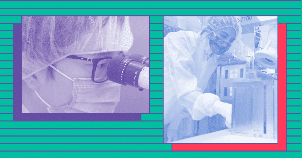
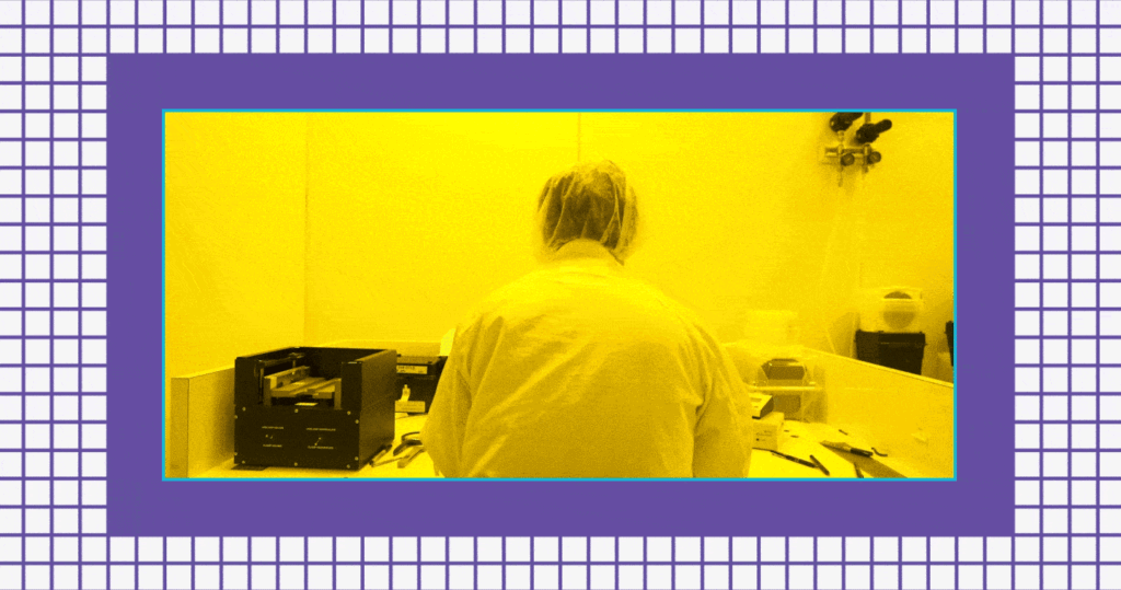
Employees often unknowingly pass by, but every day researchers on the Non-Volatile Memory (NVM) research team suit up in head-to-toe clean room attire to enter the lab. Within its walls lives a host of tools including high-powered microscopes, electron lithography beams, and deposition tools used in nanoscale R&D. Some rooms are illuminated with yellow light because the photoresists used in patterning wafers are sensitive to blue light and nanoscale projects are too small to be seen with the wavelength of regular (blue) light.
It is here that Jordan Katine, senior director of NVM memory design and fabrication, manages a team of 20 researchers, many of whom have joined the company because of the state-of-the-art lab and its opportunities. In addition, the lab often hosts researchers from universities and startups who flock to the San Jose facility for specialized equipment they wouldn’t have access to otherwise.
“My team is made up of people with different specialties because there’s different kinds of technology used to build our devices,” said Katine. “There’s lithography, etching, chemical mechanical polishing, material scientists, and more. It’s cool seeing all these experts working together.”
What’s happening in the nanoscale lab?
Nora Dávila, principal R&D integration engineer, is one such expert. She is responsible for the design of process flows used to build nanoscale devices. She explains that the lab is focused on non-volatile memory research. The lab consists of three sections: materials, processing, and testing. In the lab, researchers design, create, and test future storage innovations on 150 mm wafers.
While most of the emerging memory projects are confidential, future areas of innovation include magnetic random access memory (MRAM), phase change memory and projects for the company’s HDD, and flash businesses.
“It’s extremely exciting to do research on nanoscale technology and help accelerate it into the future,” said Dávila.
Working at the nanoscale level requires tools such as Anelva sputter deposition system and the Raith electron beam lithography tool. The Anelva system deposits materials with almost atomic layer precision. The Raith electron beam lithography tool patterns feature as small as 10 nm and electron microscopes with 1 nm resolution. These tools allow engineers to work on device components at 20 nanometers or sometimes even less.
How small are we talking?
“A nanometer is 5,000 times smaller than a red blood cell,” said Katine to give perspective. “One human hair is 70,000 nanometers wide. An atom is about a half a nanometer. We can’t use light to pattern devices at this size because the wavelength of natural light is 400 nanometers. UV light is about 100 nanometers. To work at 20 nanometers, you have to either pattern using X-rays or high energy electron beams.”
Central to the Nanoscale Lab is the electron beam lithography tool contained in a room with an isolation pad that allows the tool to be isolated from vibrations. He likens the electron beam lithography tool to a pointillism painting where an electronic beam is positioned over the wafer where you want to draw individual pixels.
The Anelva system resides in a room with a raised floor that allows the many pumping lines, process cooling water, process gases to be connected from beneath the tool.
“When you’re dealing with devices this small, you have to be able to analyze them,” said Katine.
“We have these world-class transmission electron microscopes in the Building 50 materials lab that allow us to actually see what we’re building. Because if your device is 40 atoms across, you’re not going to be able to see much with an optical microscope.”

Keeping nanoscale components clean
These intricate parts and materials require a clean room environment to keep dust, debris, and chemicals away from the components. Certain chemicals could destroy a wafer or introduce defects. In nearby buildings, where there are manufacturing assembly lines for head and media development, employees must wear full cleanroom or ‘bunny’ suits.
Western Digital was deemed an essential business early in the pandemic and the Nanoscale Lab never shut down. “A clean room is one of the safest places to be in a pandemic,” Katine said. “Your face is always covered. Your hands are always gloved. And the airflow inside the lab turns over air faster than if you were outside. So even though we’re inside, from a virus perspective it’s like being outside on a windy day. The constant ‘whooshing’ sound you hear when inside the lab is the air circulating through.”
Nanoscale lab attracts top talent
It’s the state-of-the-art clean room, access to the latest technology, and stringent safety standards that attracted Dávila and others to work in the lab. San Jose (and California) has strict safety requirements that the lab follows. For example, research labs can only store one pound of a Silane, used for chemical vapor deposition, because of its hazard classification. If a project required more, the company would have to build a separate bunker built with double-walled stainless steel to contain it.
Labs and foundries exist at several universities in California and other states, but they aren’t as advanced as this one. The Nanoscale Lab maintains multimillion-dollar tools to build components on 150-millimeter (approximately 6-inch) wafers to build devices with target dimensions typically around 20-nanometers.

Startups come to the Nanoscale Lab to build prototypes for their devices. Since building a clean room is incredibly expensive, the other options are to either go to a 300-millimeter foundry (which would be very expensive) or to a university lab.
“It’s the most cost-effective, time-efficient way to do R&D in the memory and storage space,” said Katine. “It hits that sweet spot where you’re able to accomplish something that you can’t do in the university setting, but it’s much less expensive doing R&D on 300-millimeter tools.”
When visiting startups use the lab for their own research, it’s often a joint development venture where Western Digital shares the intellectual property.
From idea to innovation
Much of the research done in the lab is classified, but many of the engineers hold patents and share their research at industry conferences and in technical papers.
“We’re working on long-term projects five to 10 years out,” said Dávila. “It’s exciting to be a part of this research at the beginning stages, to see an idea become a prototype and bridge the gap to bring that idea to fabrication and eventually mass production.”
As the storage industry moves forward, the Nanoscale Lab plays an integral role in innovation.
“As we as a collective society keep producing more and more data, we need to work on the storage technology to support it,” said Dávila. “It’s exciting to see how we can take new devices and device-physics learnings and make it into the real world.”


