Joyce Chen: The Intricate Details of Substrate Design
Details are crucial for Joyce Chen. They have to be. Chen, a senior manager of package design engineering at Western Digital, leads a team of engineers responsible for the intricacies of semiconductor packaging design. Attention to detail is just one of her traits ideally suited for the job.
Packaging design involves a series of steps to transform a semiconductor wafer into a functional product. A package in this sense is an enclosure that protects semiconductor chips within and provides a way for the chips to communicate with the larger electronic system while exhausting heat from the enclosure.
Chen’s attention to detail, work ethic, and problem-solving skills have brought her to lead system-in-package designs for Western Digital’s microSD, SD, USB, and uSD enterprise and commercial cards. She has an aptitude for inventing, which has helped create best-in-class products.
The roots of innovation
Born and raised in Taiwan, Chen is one of eight children. She describes herself as hard-working and responsible, characteristics she attributes to her father who worked as a farmer by day and a fisherman by night to support his large family.
“I only saw him for three hours every three days because at midnight he went to the beach to fish, and once he returned home, he went out to see his farm to check on the rice and the water,” said Chen.
Her father planted the seeds of hard work in Chen as she worked multiple jobs to pay for college. She was a dormitory cadre (or resident assistant) and she sold oysters at the beach. She won the Dajia Zhenlan Palace scholarship, earning the award’s highest score. She graduated from the National Yunlin College of Engineering, then earned her bachelor’s degree in mechanical engineering from Chung Yuan Christian University in Taiwan.
Before joining Western Digital, she spent five years working at Advanced Semiconductor (ASE ChungLi), the largest assembly house in Taiwan and a global tier-one assembly house. It was there that her mechanical design teacher helped her land a part-time job as a drawing machine jig in the Motorola Equipment department of the Zhongli Factory (ASE acquired Motorola ChungLi in 1999).
When she considered leaving, her manager offered her an opportunity to stay in the factory and be an equipment engineer or join a brand-new R&D department on the bonding diagram team.
She took the R&D position, but routine work didn’t satisfy her. After two years, she requested a transfer to the substrate design team, a newly formed team without any training materials.
“I thought, ‘How can I build substrate design capabilities in a short time?’” said Chen. She decided to visit the front end of the production line to learn about the process in her free time. She spoke to production operators to understand any issues from the strategic side. And she then built a design concept from die placement to routing arrangement that met production and product requirements.
Chen proved she had strong intentions and the capability to learn substrate design so the design leader asked her to supervise the team.
Her first design was for the company’s Motorola PBGA, a 27mm x 27 mm package size with more than 30 components. She spent time on the die placement components and routing arrangement based on product requirements. To meet a tight deadline, she spent two weeks and the ensuing weekends designing this substrate.
“I was so happy, there was a sparkle in my eyes,” she said.
A path in package engineering
Chen joined the SanDisk packaging engineering team in 2004. She and her manager visited Siliconware Precision Industries Co., Ltd. (SPIL), which was a second-tier assembly house in Taiwan.
Chen was surprised to see her manager’s name on the patents in the SPIL showcase room. She told her manager that she had never written an invention. Her team had a goal for each engineer to submit two innovation applications or one file per year. Her manager encouraged her to take a chance.
“He wanted us to solve problems or create new processes, products, in best-in-class packaging working with function teams including PIE (Package Integration Engineering), NPE (New Product Engineering), CPI (Chip-Package Integration), PME (Process Module Engineering), pathfinding, substrate process, and hardware,” she said.
As she worked on integrated circuit (IC) packaging, she learned new brainstorming skills from her manager. She learned how to consider changes of dimension, pattern, process, timing, structure, separation, combination, or material to create a breakthrough invention. She treated all packaging challenges, products, process development, and even product failure as an ideal chance for innovation.
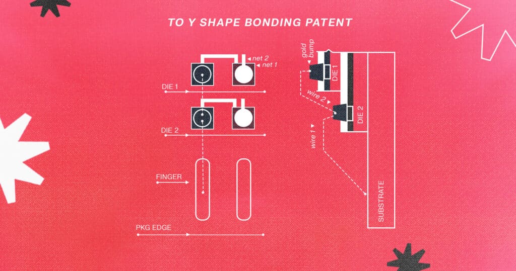
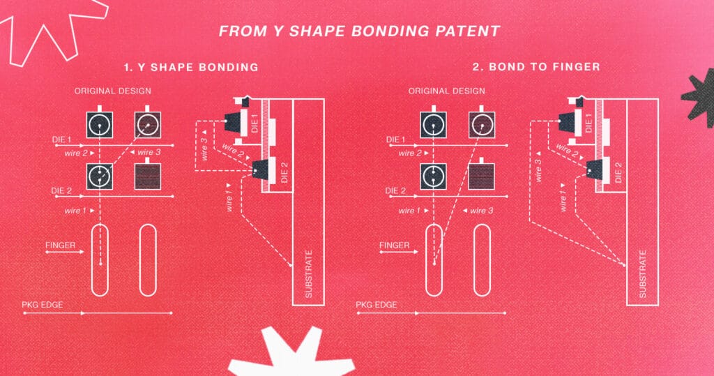
Her first invention changed the wafer mask pattern by removing the Y-shaped bonding (or longer wire) for a better connection with less risk of interference.


Fast forward 20 years and Chen has now submitted 43 inventions, 20 of which have been patented or are trade secrets. And she has propelled her teams of designers to take their first steps toward transforming ideas into innovations.
“Even if you only have basic knowledge, you can jump out of the box or do reverse thinking to create an idea. I believe anyone can be an inventor,” said Chen.
A lifelong learner
Chen is excited about her inventions. She hopes to inspire more engineers to innovate and offers advice to other inventors in the company.
“Don’t be afraid to face challenges, risks, and problems from your work,” said Chen. “This is your chance to become an inventor. Only by continuing learning, taking chances, and sharing will innovation continue. Then, you are on your way to becoming an inventor.”
Chen knows it is difficult to take the first step. She now helps each of her designers to cultivate ideas from design challenges as her former manager did—helping them become innovators. She knows the fruits of her hard work, and she is energized by knowledge.
As her father once said, “As long as you work hard in life, the black soil will turn to gold.”


