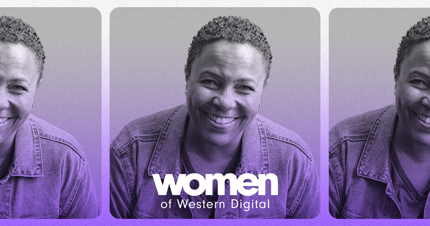
Grishma Shah thrives on creativity. Initially aspiring to be an artist or architect, Shah instead took a different route.
“I realized I don’t have to be in the arts or architecture fields to be creative,” said Shah. “You can apply creativity to anything you do.”
Today, Shah is a distinguished engineer at Western Digital. She holds more than 60 patents and sits at the center of the evolving role of flash memory, leading the company’s Future Memory Engagement team.
As Western Digital continues its legacy in flash excellence, Shah’s team is responsible for exploring and defining the next generations of NAND and the flash storage devices they serve. It is here that she connects the dots between technology options and future storage devices to meet product requirements in terms of performance, cost, and schedule.
“I work on solving very complex problems in a fast-changing environment,” Shah said. “It requires navigating different options to deliver flash technology and products that will work well many years down the line.”
Shah and her team evaluate and determine which capabilities and features are needed for each new generation of NAND. It’s a cross-functional effort where she works with leaders and stakeholders across the flash business unit, including system architecture, memory design, testing, and product marketing.
Scaling NAND
Critical to pathfinding the next generations of flash is scaling NAND to support the never-ending growth of data.
“Every application we use, every electronic item that we use generates data. From cars to laptops to digital assistants, they all require data storage and data exchange,” said Shah.
NAND scaling means packing more memory into the same area, and one key breakthrough has been 3D NAND. Analogous to building a skyscraper, 3D NAND scales by building more floors (scaling vertically), adding more rooms per floor (scaling laterally), and achieving more occupancy per room (scaling logically).
The more memory packed into the same area of a NAND chip yields higher capacities, but with each generation, density, and features of a NAND die, there are advantages and drawbacks for a storage device.
“Achieving high density will mean we can have larger capacities in a single die, but there’s a challenge in meeting performance goals with fewer dies,” said Shah. “But every time there’s a hurdle, there’s also an opportunity for innovation.”
Innovations and inventions
As a recent graduate, Shah joined SanDisk (later acquired by Western Digital) in 2006 as a NAND designer. She worked on the platform that enabled the company’s first PCIe client SSD product. It was the first time the company had an in-house controller, a technology that today is at the core of all its flash devices.
She takes pride in knowing her contributions significantly impact flash products.
Her inventions include broken wordline detection, early progress termination, and program failure handling, all of which detect defects on the fly and mitigate them. Some of these innovations were critical to enabling the company’s 2D and 3D NAND products.
Her creativity brought new concepts to flash—like “independent plane read,” an idea people initially scoffed at. “People said it was too dreamy and too complex to design,” she said.
But Shah persevered, and eventually got buy-in with help from her mentor, Dr. Yan Li. Independent plane read allowed the team to nearly double the random read score for SSDs. This feature allows four different logical pages of four planes to be read in parallel, asynchronously.
“It was a game changer at the time, and other vendors eventually adopted it as well,” said Shah. “This is a perfect example of an idea people initially ignored, but then these features became the backbone of our products.”
One of Shah’s most recent contributions was in the company’s groundbreaking CBA (CMOS directly Bonded to Array) technology, which originated when the industry shifted from 2D to 3D NAND. Shah and her team worked on identifying the right NAND configuration and feature set that would unlock the best potential of this technology in Western Digital products. This innovation, coupled with scaling advancements, enables the industry’s highest bit density 3D NAND flash memory technology, recently announced by Western Digital and Kioxia.
“I use the knowledge I’ve acquired over these years every day,” said Shah. “I know the intrinsic cell and electron levels as well as circuit-level details inside NAND. I have to understand the implications of those minute changes and impact of NAND scaling and tie it into our systems design.”
Flash-forward, memory ahead
Shah is excited for what she cites as “once-in-a-century” opportunities for flash storage with trends in autonomous vehicles, AI, the need for sustainable products, and the unstoppable growth of the zettabyte era.
“There’s an ever-growing need for memory, and it’s only going to grow,” said Shah. “You can’t keep expanding the footprint of data centers. We cannot keep building bigger and bigger data centers. That creates a need for creating smaller form factors in which memory products can be delivered.”
Shah’s team is helping define and shape those flash storage innovations; pathfinding with creativity.


